So today my FPGA board arrived! I’m excited because this means I finally get to start experimenting with actually designing all of the Athena’s modules for real now and seeing them in action.
Of course, the very first thing I wanted to do was just figure out how to program the thing and make some blinkenlights, so after accessing the website served up by the Linux core of my DE-10 Nano and sifting around the Terasic docs, I finally found the tutorial I was looking for and set about creating a new Quartus project, throwing together a simple counter, and tying one of its bits to an LED.
Not very long later, I had a blinking green LED on the board. Amazing!
Naturally, once I knew how to flash my board with a new FPGA design, it was time to start working on more complex logic. My first target: getting my SNES gamepad logic up and running.
Now, the thing about FPGAs is that, like I mentioned before, they do not run on sequential logic at their core. FPGAs are, after all, just basically reconfigurable electronic circuitry which is asynchronous by nature. However, when you’re using a language like Verilog, one thing you CAN do is design your logic to operate on a running state stored in registers. You can use registers to store state, and go down different branching logic paths on each of these clock cycles depending on that state. One very common design pattern used is state machines for when a series of events needs to take place on sequential clock cycles.
I’ll be using a state machine as the core design of my game controller module. The state machine will operate as follows:
- On reset, the game controller module will place itself in the “idle” state.
- In the idle state, the game controller module will transition into the “begin poll” state (eventually I want to have this triggered by a write attempt from the M68K, so later I will make idle be responsible for waiting for this write attempt first)
- In the begin poll state, the game controller module pulls the LATCH signal high and then transitions into the “wait latch” state
- In the wait latch state, the game controller module pulls the LATCH line low, sets up a few bookkeeping registers, and then transitions into the “read” state
- In the read state, the game controller flips the CLOCK line and, when the clock line goes low, it reads a new bit in from the DATA line into a register at current bit count, and increments current bit count.
- Finally, while in the read state, if bit count is 16 (meaning all buttons have been read), it transfers the contents of the temporary button state register into a final output register and transitions back into the “idle” state.
There’s one more thing my game module needs to do, and that’s implement a simple clock divider – the SNES controller is expecting clock periods on the order of 12 microseconds, but my 50MHz board clock has a clock period of just 0.02 microseconds! So I’ll need to slow my logic way, WAY down – by a factor of 600!
However, before I even worry about all of that, I need to get my makeshift SNES controller port wired up to my new FPGA board.
I decided to tie these lines directly to some pins on the GPIO_0 header on the Nano. CLOCK goes on pin 1, LATCH goes on pin 2, and DATA goes on pin 3 (naturally, power and ground went to +3.3V and GND pins on that header too). That ended up looking like this:
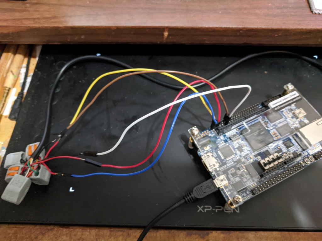
After wiring this up (twice, the second time I swapped out the jumper wires with some male-to-female ones and plugged them into a breadboard so that I’ll be able to share some of these pins such as power and ground with more than one peripheral later), it was time to start coding.
First task: forget the clock cycles. I just want to pulse the latch line and read back the state of the B button.
So I threw together a simplistic clock divider: I keep a 32-bit counter register which I increment by a constant value every global clock cycle, and a clock pulse value which I assign at the same time so that whenever that 32-bit counter rolls over, the clock pulse register becomes 1. This just left me with finding an arbitrary constant that caused the counter to roll over at a rate of around 166 KHz given my 50MHz input clock (this gives me a period of a little over 6 microseconds instead of 12 – this will still work because of the way my state machine will distribute changes across two of these cycles). This can be calculated as ( 2³² ) × ( desired-frequency / actual-frequency ). In my case this constant, truncated to an integer, was 14316557.
Then, I tossed together a simple state machine which operates whenever the clock divider above asserts a strobe (note: it doesn’t run on this strobe as a direct clock source for many reasons you can find everywhere on the net, but instead runs every clock cycle and just checks whether the strobe is asserted):
- idle: transition to begin poll
- begin poll: pull LATCH line high, transition to wait latch
- wait latch: pull LATCH line low, transition to idle
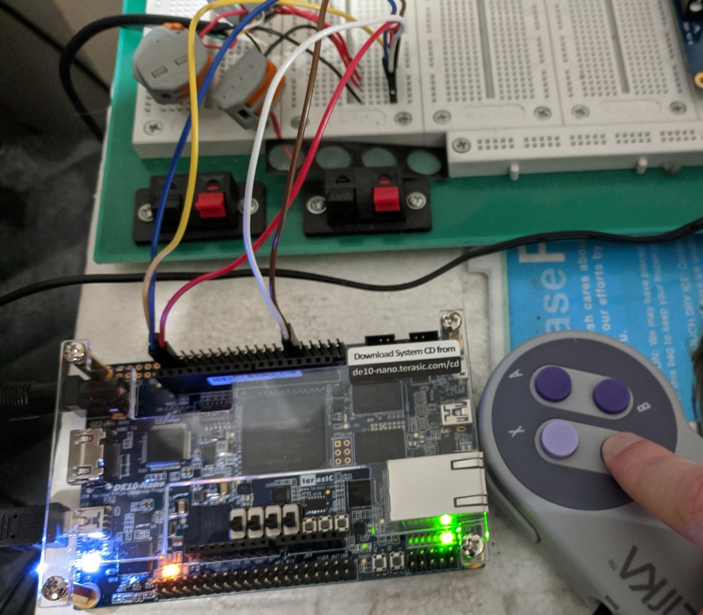
I wired this up to a module which ties an LED directly to the state of the DATA line so I could see whatever the controller latched, compiled it, and loaded it onto my FPGA.
Lo and behold, the LED was lit and then turned off whenever I held the B button down. Huzzah! Note that the DATA line is active-low, so this “backwards” behavior is to be expected.
After that, it was just a matter of wiring up the rest of the state machine as I outlined above in this post and also inverting the incoming button signals. Then I got my gamepad module to expose the controller state as a 16-bit wire array, and tied some LEDs to the first and second bits of that wire array. Success! Pressing the B button lights up one of the LEDs, and pressing Y lights up the other!
I’m very excited to have this working as expected so quickly. Now that I’ve gotten this part working, I think one of my next tasks will be throwing in the FX68K core and seeing if I can replicate a “free-running” test with it (feeding it 0 on its data pins and tying an LED to one of its address pins so I can watch the LED strobe while the CPU cycles through its entire address space executing a dummy instruction).
And after that? Who knows!
