Featured

Introducing Athena: My FPGA retro game console project

Normally, I’m a software engineer. In particular, I specialize in architecting netcode for games. A few weeks ago, I departed a job doing just that at Super Bit Machine – the game I worked on for two years was successfully launched and I’m quite proud of the work I did on it.

That said, having most of December off gave me some time to work on personal projects and I ended up returning to an old hobby: messing around with electronic crap that I barely understood and probably have no business messing with.

In particular I’ve been tinkering with a technology I find absolutely fascinating: FPGAs.
FPGAs (Field Programmable Gate Arrays) are so interesting to me because not only is it a single simple chip that can be reprogrammed into almost any digital logic circuit you could possibly dream up, it also gives you a way to design your digital logic with very high-level concepts: using a language like Verilog, you can express your logic with high level syntax and let Verilog do the work of putting all of those low-level logic gates together for you (adders, comparators, multiplexers, etc).

However, FPGAs are also a little odd for me to mentally grasp. Remember, I’m a software engineer by trade. In computers, everything operates mostly sequentially. The hardest problems for us to solve are when they don’t – generally, multi-threaded code that allows multiple pieces of code to run at the same time and possibly try and interact with each other in unpredictable order can be some of the toughest designs to tackle.

By contrast, absolutely nothing in an FPGA runs sequentially unless you design it to. And yet I can’t resist the appeal of trying to work with them anyway. And that brings me to this project: Athena.

Athena is a little project of mine to implement a game console on an FPGA. Crazy (at least for me)? Possibly. But I frequently learn by tossing myself into the deep end of the pool so to speak, so honestly I’m not too worried.

Now, onto the design of the Athena.

Athena will be designed as a very retro console, aiming for something that would feel at home in the late 80s to early 90s. Think the 16-bit era of gaming. I want to make use of chips that would actually have been available for a console of the time, and this brings me to one of the reasons FPGA is a fantastic choice: I can grab old IC implementations mostly off-the-shelf and toss them into my FPGA design without having to scour Ebay for old chips that have been out of production for years. I can also custom design my own bespoke modules for when I need something that I just can’t find off-the-shelf.

That said, here’s what I’ve decided on for Athena:

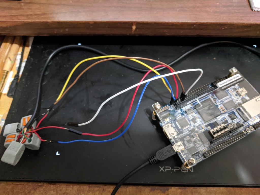
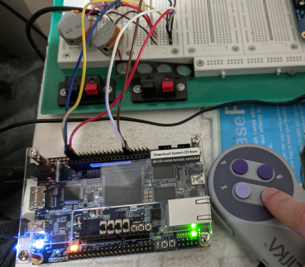
  • I will be using the Terasic DE10-Nano as the development board for this project. To be honest, I was more than a bit inspired by MiSTer’s use of this board for their purposes. I figured if the board was good enough for a MegaDrive core, it should be good enough for me!
  • The heart of the console will be a Motorola 68K CPU, clocked at 12.5 MHz (exactly 1/4 the board’s 50MHz clock speed. I was, and still am, tempted to clock it at 25MHz instead but that feels a little less authentic to me).
  • 64KB of SRAM will be available to the CPU for code storage and general RAM.
  • A bespoke video generator module will be responsible for driving 320x240p@60Hz video output, supporting two scrolling tilemap layers, up to 128 hardware sprites (up to 20 per scanline), and 256 colors per scanline with 4 bits per RGB channel. As the DE10-Nano has a video transmitter built-in, this will be done over the HDMI out. The video generator has 32KB of SRAM dedicated to storing color palettes, image data, tilemap data, and miscellaneous registers.
  • A YM2151 chip and a bespoke 4-channel PCM chip will together be responsible for outputting 44.1KHz stereo 16-bit audio over the HDMI out. The 4-channel PCM chip will have 32KB of SRAM dedicated to storing 8-bit unsigned PCM samples. Both the YM2151 and the PCM chip will be memory-mapped into the M68K bus. The audio sample RAM will not, but more on that later.
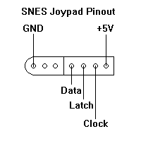
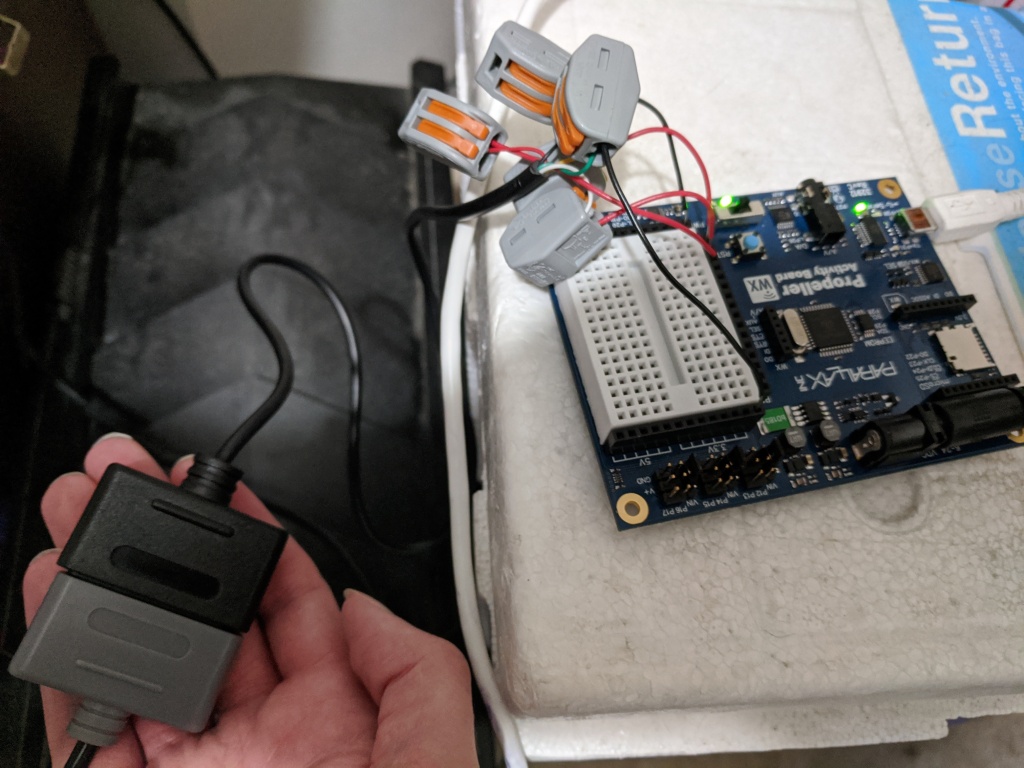
  • The Athena will support two controller ports pin-compatible with the original SNES game controller, memory-mapped into the M68K peripheral bus with a serial-to-parallel interface on top to simplify interacting with them.
  • A bespoke DMA controller will simplify interacting with memory that isn’t directly attached to the M68K bus – namely, the video RAM, and the audio sample RAM. Code running on the M68K will ideally be able to just signal a memory copy from main RAM to either VRAM or audio sample RAM, and the DMA controller will handle temporarily disabling any modules it needs to for the duration of the copy to prevent bus contention issues.
  • The Athena will support the DE10-Nano’s onboard SD card reader, memory-mapped directly into the M68K peripheral bus with a serial-to-parallel interface on top to simplify interacting with it. An onboard bootloader ROM attached to the M68K bus will be responsible for loading a default boot program off of the SD card into the main RAM, making the SD card slot act essentially as the Athena’s game cartridge port (games can also use their own logic to drive the SD card slot, which could potentially be used for things like loading assets and storing game saves)

So, for a little while, I’m going to be chronicling my adventures in trying to design this daunting behemoth of a design. Will it end in absolute failure? Will it end in a cool working retro console? Who knows!

I guess we’ll see!

EDIT (12/24/2019 5:21 PM)
– It occurs to me that the SD card reader built into the Nano board CAN be controlled from the FPGA core, buuut it’s supposed to contain files that are important for both the HPS as well as the files to initialize the FPGA core on boot, so I’m a little more hesitant to use it as a makeshift cartridge slot now. Actually, I already have a separate SD card reader breakout board on hand, so I think I’ll just use that instead and wire it up to some GPIO pins.

On FPGA memory block optimization

So this is something that bit me in the ass pretty hard recently until someone far more experienced than me on Twitter was able to help me through optimizing my crappy code, and so I figured I’d make a blog post about it.

In Verilog, there’s a concept of a memory. A memory is basically an array of registers, it looks like this:

reg [n-1:0] myMemory [0:m-1];

It’s called a memory because, well, that’s pretty much exactly what it looks like: a big array of n-wide registers accessible by a memory address from 0 to m – 1. While this looks like a plain old array, there’s more to it than that and this is what gave me some heartburn.

The thing is, most synthesis software is actually pretty good at optimizing this. Normally, if they can get away with it, they will actually implement that above “myMemory” register array in on-chip RAM blocks. It’s fast, it doesn’t take up logic slices, and generally preferable for when you’ve got LOTS of those registers.

The problem is if you aren’t careful with how you access them, you can very easily break your software’s ability to prove that it CAN implement it in on-chip RAM, and it will instead resort to things like implementing as a HUGE array of flip-flops. This is exactly what I was experiencing while I was working on the VCP.

Thing is, my VCP draws one line at a time. Rather than try and have my VCP draw everything on-demand right as the pixel is needed, I used linebuffers so that my VCP can just prepare a whole line of pixels in advance. Actually, several linebuffers are used in my VCP implementation – multiple tile and sprite plane buffers are prepared and then all muxed together into the final linebuffer according to layering rules.

Here’s the thing about that: The way I had implemented my VCP, a single 16-bit word read from VRAM encodes four pixels, each a 4-bit index into a 16-color row in the color palette, so what I was doing was just blasting all four pixels directly into the target line buffer as soon as they were read from memory.

This was apparently a horrible idea.

In order for Quartus to be able to infer on-chip RAM, it needs to be able to safely infer that it can implement it using a single address and data port for the RAM – and that means only one write per clock cycle. Doing multiple writes like this completely violates that. Quartus instead resorted to huge flip flop dumps. That took up easily 60% of my FPGA’s logic resources. Bad bad bad.

So instead, I had to completely restructure how the writes were done. My approach was to stick the 16-bit word into one buffer (which, itself, could be synthesized as RAM due to only one write per cycle) and then read one 4-bit value per clock cycle into the target line buffer (once again, can be synthesized as RAM due to one read -> one write per clock cycle). This took a bit of effort and a bit of proving that nothing overlapped in bad ways, but I finally did get it working. New logic utilization: 15%. Whew! That’s WITH two independent scrolling tilemap layers and 128 sprites. I also haven’t fully optimized everything – I’m pretty sure the tile fetch buffer (which fetches 41 tiles each scanline) is being inferred as flops right now, as is the color palette – but this is still a huge savings and let me continue on with the project without worrying about running out of room just yet.

Anyway, let that be a lesson: pay attention to your memory usage patterns in Verilog! It just might save you a huge amount of flops.

Day 6: The VCP, VRAM, & Clock Domain Issues

So over the last couple of days I started work on the video co-processor (from here on I think I’ll refer to as the VCP) of the Athena. The goal of this co-processor is to get two independently scrolling tilemap layers, 128 sprites, and 256 onscreen colors.

This turned out to be a bit of an adventure. Not the least of my problems was trying to find a way to allow the CPU and the VCP to both access VRAM. The thing is, I need to let the CPU be able to write into VRAM so that we can change color palettes, scroll tilemap layers, modify the sprite table, upload image data and tilemap data, etc. And the VCP needs to be able to read from VRAM while drawing. And, unfortunately, a single RAM module can only do one of those things at a time.

My first attempt was to try and stick a priority arbiter in front of the VRAM chip. The idea was that I would use the DTACK line of the CPU to implement a sort of blocking wait state – if the VCP and the CPU both wanted to access VRAM at the same time, the arbiter would grant the VCP’s request and de-assert the CPU’s DTACK line which causes the CPU to halt, until the VCP was done and the DTACK line was re-asserted.

This failed miserably. The CPU mostly just locked up completely. Maybe I just didn’t implement it correctly, but I decided to try a different approach anyway.

My next attempt was to use a control port on the VCP. The idea is very similar to the way VRAM writes work on the Sega Genesis (and, probably, for extremely similar reasons): the CPU would write into an address and data port on the VCP, and the write a value into a control port to signal a write request. The VCP is then free to schedule this to be processed whenever it isn’t already interacting with VRAM.

So I set about trying to implement this and running into various odd problems, and that’s when I realized something pretty crucial: my CPU and my VCP run on different clocks, and I was running into clock domain crossing issues.

What is clock domain crossing? Basically, if you have one signal tied to one clock, and a process on another clock trying to sample that signal, you can end up with some very strange results in real hardware. There are various ways to deal with this problem. For very simple cases, you can just feed a value through a chain of two or three flip-flops on the target clock to (relatively) safely synchronize the value (the chance of an error is never mathematically zero in this case, but it is very very near zero). However, in this case I went with a different approach: a dual-clocked FIFO queue.

A FIFO queue is of course easy to grasp if you’re a software developer: you can enqueue multiple values, and then later dequeue them in the order they were enqueued. In this case, there’s a special kind of FIFO queue that’s specifically designed to run on two clock signals – one for reading, and one for writing, and as a result provides a way of synchronizing values from one clock domain to another.

The nice thing is that Quartus provides me with a built-in customizable FIFO construct that allows for this exact setup, so I’ll just go ahead and use that. I decided to make the FIFO width 32 bits – when I enqueue values onto this FIFO from the source clock domain (the clock my CPU runs on), I merge the 16-bit address and 16-bit data ports into one single packed 32-bit value. On the receiving end, when I dequeue values from this FIFO on the destination clock domain (the pixel clock my VCP is running on), I split them back out and use them to generate VRAM address and data port values. My FIFO also provides a write full signal, so I also decided to wire things up so that reading from the control port mentioned previously yields a 0 or 1 value, 0 if the FIFO still has room, 1 if it has become full. This is used so that on the CPU side you can manually check if a write has filled up the FIFO and wait until it empties a bit before adding more write requests. This generally shouldn’t happen though, since the CPU is running at 12.5MHz and the pixel clock is 25.127MHz (so it shouldn’t be possible for the CPU to outstrip the VCP’s read rate)

So that solves getting data from the CPU into VRAM, but what about actually rendering?
Well that, too, was an adventure.

At the moment, I’ve only got one single tilemap rendering, but I should be able to build on this and implement the rest of the VCP rendering features.

In the end, what I went with was a state machine that works like this:

  • In STATE_idle, wait for a Horizontal Interrupt signal from the VGA generator. On receiving the signal, latch the current state of the scanline counter, flip the currently active line buffer, and transition to STATE_draw_line
  • In STATE_draw_line, fill the current line buffer with the first color entry in the color palette and set up the first read for the next clock cycle (reads the tile intersecting the leftmost pixel of the line from the tilemap address given in tile plane A’s registers), transitions to STATE_fetch_tile_row
  • In STATE_fetch_tile_row, the results of the read set up in the last cycle are fetched from VRAM into a row of tile data registers, sets up the next read address, and loops back into this state fetching one tile per clock cycle until 41 tiles have been fetched. It then sets up a VRAM read for the pixel data of the first tile and transitions into STATE_draw_tile_row
  • In STATE_draw_tile_row, the results of the read set up in the last cycle are fetched. Each word encodes four pixels of data, indexing one 16-color row of the color palette at a time, so four pixels are then blit into the current line buffer, the next four pixel VRAM read is set up, and it loops back into this state until all 41 tiles have been blit into the current line buffer. It then transitions back into STATE_idle.

It took a little bit to get this working properly, but in the end I did succeed. You can see the results below:

The other thing I did in the above video was get external interrupts working so that I could make use of a vblank interrupt. This isn’t super tough if you read the M68K data sheets but I’ll outline the basics: first, you need to set the Status Register to indicate which interrupts you want to handle (by default it’s 7, which indicates that interrupts 6 and below will be ignored). I set the the interrupt mask portion of this to 0 so that all interrupts would be handled. Next, to assert a priority, you need to set the 3 IPL lines to encode an interrupt priority (you can encode a value between 1 and 7). After that, you check the 3 FC output lines. If they become 111, you know the CPU is about to handle the interrupt, and the interrupt it’s about to handle has been placed on the lowest 3 bits of the address lines. You can use that to de-assert that particular interrupt request. I personally put together a couple of modules to help with latching interrupt requests and unlatching interrupt requests in response to the interrupt acknowledge from the CPU.

So, what’s next? Well, since I’ve got one tilemap done, next I’ll probably work on sprite rendering, and then extend this to support multiple tile and sprite layers. And then it’ll probably be onto the audio subsystem!

Day 5: HDMI and VGA

So today I decided to start working on getting some video out of my board.

My DE-10 Nano comes with an HDMI port and a video encoder chip built right into it, so that makes a pretty obvious choice of video output. My first order of business was just to see if I could get my monitor to recognize a signal and display a black screen.

After reading through the datasheets of the included ADV7513 HDMI transmitter chip, I knew that first I had to program a pretty hefty number of registers over I2C to initialize my video output. At first I tried using a Verilog I2C master module interface to do this, but after trying unsuccessfully to get it to do absolutely anything at all in a simulator, I suddenly became very lazy and just copy pasted the HDMI config bits from the Nano’s own demo examples.

I wasn’t entirely sure if this worked, because my monitor didn’t seem to recognize any valid signal at this point, but I decided maybe the HDMI transmitter chip just needed an actual video signal and started working on that.

The cool thing about the ADV7513 is that although it outputs HDMI, what it takes as input is actually just a standard VGA video signal – right down to the hsync, vsync, active area, and pixel clock timings. The good news is generating a VGA signal is extremely easy. And because I’m driving this chip with a VGA signal, it would be trivial to modify my board to output a separate analog VGA signal later with almost no changes at all. And even further, because VGA timings are to some extent a slight modification of existing broadcast standards, it might even be possible to extend my board to output NTSC composite video later on! But that’s a problem for future me.

Anyway, back to generating a VGA signal. What I want to generate is a 640x480p@60Hz signal (the video co-processor will actually output a 320×240 image, but I will implement line-doubling and double each pixel horizontally to stretch this to the full screen). Given this, the VGA spec wants a full frame of 800×525 – 160 pixel clocks before the start of each visible scanline contains the front porch, a sync signal, and the back porch, and 45 scanlines after the end of the visible screen will contain an additional front porch, sync signal, and back porch. These offscreen areas are used to synchronize the signal horizontally and vertically (if you’re familiar with NTSC this may look very similar!)

VGA framerate is also 60÷1.001 (not precisely 60! this came from legacy NTSC standards once again), and that means I need to display 800 × 525 × ( 60 ÷ 1.001 ) = ~25175000 pixels per second. Therefore my pixel clock will be 25.175 MHz.

Unfortunately this isn’t a nice multiple of the 50MHz board clock, so I’ll make use of one of the Nano’s built-in PLLs instead to give me a nice precise fractional clock divider. Configuration of these is pretty simple, I just asked Quartus to instantiate the PLL Intel FPGA IP, chose Fractional-N Pll, and picked 25.175 as my output clock.

With that I threw together a quick VGA module, and (after a few attempts where I forgot to wire up the hsync, vsync, and data enable signals properly) that was apparently the missing piece. Once I was sending a VGA signal, the monitor seemed to accept the signal and stay on, albeit completely black. This also means the HDMI config bits I copied over were working fine!

A bit of fiddling later and I was able to prove that it was able to display colors and even a little grey box:

Now that I’ve got a video signal, my text task is to start working on the video co-processor!

Day 4: The memory bus and a running CPU program

So last time I got a Motorola 68K up and running, cycling through its entire address space and attempting to execute a dummy instruction. However, in order to get the CPU running an actual program, I need to hook up an actual bus to it.

I ended up having to do a hell of a lot of trial and error and poring over data sheets cross referencing signal descriptions to get this working. In the end, I settled upon a handful of signals on the 68000 as being the interface for my bus: RW, LDS, UDS, A23-A1, and D15-D0. These signals are as follows:

  • RW: Indicates whether the 68000 is currently in a read or a write cycle. 1 if reading, 0 if writing.
  • LDS: 0 if the 68000 wants to read/write D7-D0, 1 if those pins should be ignored.
  • UDS: 0 if the 68000 wants to read/write D15-D8, 1 if those pins should be ignored.
  • A23-A1: The address the 68000 wants to read from or write to.
  • D15-D0: Bidirectional data pins to connect to each device on the bus.

With that settled on, I also need a way of being able to put multiple devices on the same bus. The way I’ll do this is by allocating some number of bits of the address pins to a demultiplexer, this demultiplexer will feed individual enable lines to all devices on the bus and each of those devices will use the enable line to determine if it needs to suppress or enable operation.

In the end, I went with using A23-A17 as input to the demultiplexer (which will allow me to connect up to 128 different devices on the bus), and using the remaining A16-A1 as an address passed to each device on the bus (allowing each device to address up to 65535 16-bit words of data, giving 128KB per device).

With the bus interface out of the way, it’s time to hook up a ROM to this CPU and see if I can get it executing some real instructions.

My ROM is really simple actually:

module ROM #(
	parameter ROM_PATH = "",
	parameter ROM_ADDR_BITS = 8
) (
	input wire				I_CLK,
	input wire				I_ENABLE_N,
	
	input wire [15:0]		I_ADDR,
	input wire				I_RW,
	input wire				I_UDS,
	input wire				I_LDS,
	output wire [15:0]	O_DATA
);

localparam ROM_SIZE = 1 << ROM_ADDR_BITS;
localparam ADDR_MASK = ROM_SIZE - 1;

reg [15:0] mem [ROM_SIZE];
reg [15:0] out;

// if chip select is asserted and I_RW is read, set O_DATA to output data
// otherwise, set 0 to let it be or'd together with other bus devices
assign O_DATA = I_ENABLE_N ? 0 : ( I_RW ? out : 0 );

initial begin
	$readmemb( ROM_PATH, mem );
end

// note: we actually need this clock cycle setup because otherwise Quartus fails to infer block RAM
always @(posedge I_CLK) begin
	out <= mem[I_ADDR & ADDR_MASK];
end

endmodule

All this really does is gives me a handy module I can instantiate with a path to a memory initialization file and a configurable power-of-two size and adds a read-only. It’s also structured so that Quartus is able to deduce that it should instantiate it using on-chip block RAM rather than using a bunch of flip-flops.

Connecting this is very simple, I can just feed it my global 50MHz clock, one of the enable lines from my bus demux (I picked 0 because that puts this ROM at $000000, which will be the very first address the CPU tries to read), and the A, RW, LDS, and UDS lines from the CPU. I also set the CPU’s input data lines to this module’s O_DATA lines.

Next, I need some code to initialize this ROM’s memory with. I used Easy68K to put together a small program containing the 256-byte interrupt table the 68000 expects as well as a simple loop that’s just an infinite nop loop (a label, a nop, and a jump back to the label), plus a C# utility that could convert the final binary ROM file into the format expected by readmemb.

Watching this from a simulator showed exactly what I had hoped to see: the CPU looping over the same two instructions (the NOP and the JUMP).

My next goal was to add a test bus device that could take a value write and store it in a register, as well as output the current value of that register so I could hook it up to some LEDs on the actual board. I hooked this device up to bus enable line 127, putting it at address $FE0000, and then changed my ROM code to write $BEEF into that test device.

Once again, this worked pretty much as I expected: the CPU issues a write cycle and selects device 127 with the value $BEEF on its data pins, and my test bus device takes the value as expected. Good!

From there, it didn’t take very much time to hook up some actual work RAM to the CPU. My RAM module works almost identically to the ROM module above, except I added a write cycle and also added support for reading/writing individual low and high bytes. I instantiate a 64KB RAM module and hook it up to bus enable 1 (which puts work RAM at $020000). I tested it by writing a value to the beginning of work RAM and then reading it back, as well as pushing a value onto the stack and popping it off (I modified the interrupt table to put the initial stack pointer at the end of work RAM).

That left me with one more task: get code running on my CPU to interface with my gamepad serial interface.

This involved writing a bus interface that would take my existing serial controller and interface it with the memory bus to allow the CPU to interact using just memory reads/writes. The plan is this: a write to $100000 relative will cause the gamepad to enter the polling state. A read from $100000 will return whether or not the gamepad is currently busy polling. A read from $100002 will return the last known state of player 1’s gamepad, and a read from $10004 will return the last known state of player 2’s gamepad.

After a bit of wiring, I went ahead and instantiated the gamepad module in my testbench. I also changed my ROM code to read the gamepad as follows:

  • Write a value to $100000. Any arbitrary value will work.
  • Reads back from $100000 in a loop and waits for the result to become 1 (indicating that the gamepad module has acknowledged the read request and entered the polling state)
  • Reads back from $100000 in another loop waiting for the result to become 0 (indicating that the gamepad module has finished polling the gamepad state)
  • Reads a value from $100002 and writes the result to my test bus device so that later I’ll be able to replicate this test on hardware and see the result on the LEDs for debugging.

Now, I should note that my first attempt at this revealed some amusing errors. First of all, I generated a read signal in my gamepad bus interface by checking if the CPU was in a write cycle. Unfortunately I completely forgot to check if the gamepad bus interface was actually, y’know, selected by the CPU. Which meant that any write, anywhere at all, would cause the gamepad module to enter the polling state. Whoops.

My next mistake was testing the wrong bit of $100000 when checking for the busy flag. I accidentally tested the second bit and reversed my comparisons, which caused the CPU to hang forever waiting for the second bit to become 1 (which it never did).

My next mistake was forgetting to actually tie the gamepad bus interface’s data output into the CPU’s data input. This caused the CPU to hang while wait for the busy flag to become 1, which it never did because the input was all 0s. Whoops.

My last mistake was reading from $100001 instead of $100002 for getting player 1’s gamepad state. That triggered a bus address exception because I tried to read a whole word on a non-word-aligned address, although I could see from the logic analyzer that it had jumped to my defined interrupt handler in the interrupt table as a result, so at least I know that works!

But, finally, at long last, I saw my code polling for gamepad state in a loop and writing the result out to my test bus device. It was time to program this onto the real thing!

And it works!

The result is you can see the states of the B, Y, Select, Start, and D-Pad buttons on the lights on the board. Now, I know it looks precisely the same as my previous gamepad FPGA experiment, but this time it’s driven by a running CPU which proves to me that my CPU is up and running real code and interacting with bus devices. Excellent!

Now that I’ve got this done, I think my next goal will be to start working on the other components of the game console. Perhaps the video encoder next?

Day 3: Free-running a Motorola 68K

So today I set about getting a Motorola 68K up and running on my FPGA board. My goal was relatively simple: just get an M68K working, fed dummy 0 values on its data pins and tying the top two bits of its output address pins to a pair of LEDs. As the M68K runs, it should cycle through its entire address space trying to read instructions from the data bus and cause my LEDs to blink at some regular interval as a result.

Now, I’m a lazy guy, and I didn’t want to have to reimplement a whole chip from scratch in Verilog if someone else had already done the work, so I ended up going with the FX68K. It’s pin-compatible and cycle accurate to the original M68K so it seemed like a good pick.

The first thing I did, after dropping the files into my Quartus project, was put together a simple wrapper module (I just called it CPU_fx68k). Its only real job is to take an input 50MHz clock and do the clock division work. Note that the FX68K needs three signals for proper cycle operation: the clock signal (my 50MHz clock), but also phi 1 and phi 2. The idea is that the CPU will divide a single CPU clock cycle into two phases, and phi 1 and phi 2 will signal these phases to execute (and should never be asserted at the same time). Therefore in my case this gives a maximum speed of 25MHz, the result of interleaving phi 1 and phi 2 on my 50MHz clock. In my case I will actually be running it at 12.5 MHz, the result of dividing my 50MHz clock by four (for every four clock cycles, phi 1 will be asserted on the first, phi 2 will be asserted on the third, and on the second and fourth clock cycles neither will be asserted).

This was simple enough, it was just a simple four-bit counter register and some wire assigns for phi 1 and phi 2. My next task was to modify my reset signal generator. I already had it generating a good reset signal (I had verified this both in simulator and on hardware), but for the CPU I also wanted a cold start signal. This wasn’t very tough either, it required a bit of finagling to make sure signals lined up the way I wanted them to (I’m not sure if having the cold start signal last for one cycle longer than the reset signal would be a problem, but I made sure to eliminate the delay anyway just in case) but was pretty straightforward otherwise. Final behavior: Powering on or reprogramming the FPGA asserts a reset and cold start signal momentarily, and then from that point onward pressing one of the key switches on the board causes only the reset signal to be re-asserted (but not the cold start signal). Cool. Next task.

The next thing I did was put together a testbench for the CPU. Essentially I want to replicate the free-running test I will be doing on hardware later, but in simulation where I can watch the address pins counting up over time. Once again, this proved to be no real issue. Things mostly just worked as I expected.

That meant there was only one thing left to do: instantiate the CPU in my top module and program it onto the real thing.

So I instantiated it, wired up the necessary signals, set up some dummy values in an initial block (set DTACK to 0, de-assert any bus request or bus acknowledge lines, set input data lines to 0, etc), hit compile, and programmed it onto my FPGA.

Aaaand…… nothing. No lights. Hm.

I played around with which bits the lights were tied to, maybe they were just blinking too slowly? But nothing seemed to work. At some point I left them on 15 and 16 and focused my attention elsewhere. I did some googling online to see if maybe the readmemb commands for the CPU’s nano code ROM weren’t synthesizing correctly, didn’t get much traction on that besides reading that Quartus should be able to handle it just fine (and it wasn’t giving me any errors that would indicate it was failing to read the files somehow).

Then I saw my initial block setting the CPU’s input pins and, on a whim, decided to switch it out for an always block.

And then both LEDs lit up completely. Aha! That’s something! They didn’t appear to be blinking, mind you, until I hit the reset button on the board and noticed that they would randomly change states when the button was pressed (either both would suddenly brighten up, only one would be lit, the other would be lit, or both would turn off) and realized that actually they were blinking, but so fast that I couldn’t see them with my naked eyes and pressing the button basically halted the CPU and preserved whatever was on the address pins when I hit the button. And that meant success!

To verify, I just changed the LEDs to be tied to bits 22 and 23 of the address and recompiled and, lo and behold, blinking lights! To make a slightly better visual, I decided to add in the rest of the LEDs and tie them to more address bits so I could snap this photo.

An array of lights resembling a binary counter as the CPU cycles through its address space trying to fetch instructions

I’m very excited to see these simple blinking lights, as it means I now have a working 16-bit CPU at my disposal.

As for my next task? I might try and see if I can wire up a simple bus interface and get the CPU running some real code with a little baked-in ROM. Maybe even see if I can put together a little debug module to let me see some bus writes from code running on the CPU.

Day 2: FPGA time!

So today my FPGA board arrived! I’m excited because this means I finally get to start experimenting with actually designing all of the Athena’s modules for real now and seeing them in action.

Of course, the very first thing I wanted to do was just figure out how to program the thing and make some blinkenlights, so after accessing the website served up by the Linux core of my DE-10 Nano and sifting around the Terasic docs, I finally found the tutorial I was looking for and set about creating a new Quartus project, throwing together a simple counter, and tying one of its bits to an LED.

Not very long later, I had a blinking green LED on the board. Amazing!

Naturally, once I knew how to flash my board with a new FPGA design, it was time to start working on more complex logic. My first target: getting my SNES gamepad logic up and running.

Now, the thing about FPGAs is that, like I mentioned before, they do not run on sequential logic at their core. FPGAs are, after all, just basically reconfigurable electronic circuitry which is asynchronous by nature. However, when you’re using a language like Verilog, one thing you CAN do is design your logic to operate on a running state stored in registers. You can use registers to store state, and go down different branching logic paths on each of these clock cycles depending on that state. One very common design pattern used is state machines for when a series of events needs to take place on sequential clock cycles.

I’ll be using a state machine as the core design of my game controller module. The state machine will operate as follows:

  1. On reset, the game controller module will place itself in the “idle” state.
  2. In the idle state, the game controller module will transition into the “begin poll” state (eventually I want to have this triggered by a write attempt from the M68K, so later I will make idle be responsible for waiting for this write attempt first)
  3. In the begin poll state, the game controller module pulls the LATCH signal high and then transitions into the “wait latch” state
  4. In the wait latch state, the game controller module pulls the LATCH line low, sets up a few bookkeeping registers, and then transitions into the “read” state
  5. In the read state, the game controller flips the CLOCK line and, when the clock line goes low, it reads a new bit in from the DATA line into a register at current bit count, and increments current bit count.
  6. Finally, while in the read state, if bit count is 16 (meaning all buttons have been read), it transfers the contents of the temporary button state register into a final output register and transitions back into the “idle” state.

There’s one more thing my game module needs to do, and that’s implement a simple clock divider – the SNES controller is expecting clock periods on the order of 12 microseconds, but my 50MHz board clock has a clock period of just 0.02 microseconds! So I’ll need to slow my logic way, WAY down – by a factor of 600!

However, before I even worry about all of that, I need to get my makeshift SNES controller port wired up to my new FPGA board.

I decided to tie these lines directly to some pins on the GPIO_0 header on the Nano. CLOCK goes on pin 1, LATCH goes on pin 2, and DATA goes on pin 3 (naturally, power and ground went to +3.3V and GND pins on that header too). That ended up looking like this:

I know this screenshot shows the controller wired to +5 instead of +3.3. Don’t worry, I noticed this before plugging in an actual controller and fixed it shortly after taking this photo.

After wiring this up (twice, the second time I swapped out the jumper wires with some male-to-female ones and plugged them into a breadboard so that I’ll be able to share some of these pins such as power and ground with more than one peripheral later), it was time to start coding.

First task: forget the clock cycles. I just want to pulse the latch line and read back the state of the B button.

So I threw together a simplistic clock divider: I keep a 32-bit counter register which I increment by a constant value every global clock cycle, and a clock pulse value which I assign at the same time so that whenever that 32-bit counter rolls over, the clock pulse register becomes 1. This just left me with finding an arbitrary constant that caused the counter to roll over at a rate of around 166 KHz given my 50MHz input clock (this gives me a period of a little over 6 microseconds instead of 12 – this will still work because of the way my state machine will distribute changes across two of these cycles). This can be calculated as ( 2³² ) × ( desired-frequency / actual-frequency ). In my case this constant, truncated to an integer, was 14316557.

Then, I tossed together a simple state machine which operates whenever the clock divider above asserts a strobe (note: it doesn’t run on this strobe as a direct clock source for many reasons you can find everywhere on the net, but instead runs every clock cycle and just checks whether the strobe is asserted):

  • idle: transition to begin poll
  • begin poll: pull LATCH line high, transition to wait latch
  • wait latch: pull LATCH line low, transition to idle

I wired this up to a module which ties an LED directly to the state of the DATA line so I could see whatever the controller latched, compiled it, and loaded it onto my FPGA.

Lo and behold, the LED was lit and then turned off whenever I held the B button down. Huzzah! Note that the DATA line is active-low, so this “backwards” behavior is to be expected.

After that, it was just a matter of wiring up the rest of the state machine as I outlined above in this post and also inverting the incoming button signals. Then I got my gamepad module to expose the controller state as a 16-bit wire array, and tied some LEDs to the first and second bits of that wire array. Success! Pressing the B button lights up one of the LEDs, and pressing Y lights up the other!

The green LED in this picture, in the lower right corner of the board, lit up as I press the Y button on the controller.

I’m very excited to have this working as expected so quickly. Now that I’ve gotten this part working, I think one of my next tasks will be throwing in the FX68K core and seeing if I can replicate a “free-running” test with it (feeding it 0 on its data pins and tying an LED to one of its address pins so I can watch the LED strobe while the CPU cycles through its entire address space executing a dummy instruction).

And after that? Who knows!

Day 1: SNES Gamepad Protocol Tinkering

Continuing my series of talking about my adventures in building an FPGA game console, today I’ll talk about how I familiarized myself with the SNES gamepad serial protocol and got a working physical hardware prototype of being able to query the button states.

Now, unfortunately, my FPGA board still hasn’t arrived (it’s scheduled to arrive tomorrow according to UPS), so until then I can’t do much actual testing of FPGA-related things – aside from running simulated testbenches I suppose. However, I do have a Propeller Activity Board WX on hand, so I decided to do some prototyping there to make sure I knew how to talk to the gamepad and make sure I could wire things up right.

The first thing I did was purchase an after market SNES gamepad in addition to an extension cable. I snipped open the extension cable and used a multi-meter to test each wire inside and write down how each one mapped to the pins in the front-facing part that the controller would plug into. I did this to an extension cable rather than the controller itself so that I wouldn’t have to cannibalize a controller – yay reusability!

So, as for the pinout, they’re actually really simple. There’s only five wires I care about, and they are mapped as follows:

Now, +5V and GND are obvious. That leaves me with three IO lines to worry about: Clock, Latch, and Data. What do these do?

It turns out the inner workings of a SNES controller are actually dead-simple: nothing more than a couple of shift register ICs. The first step to getting the button states is Latch: pulsing Latch high and then low, for a period of at least 12us, causes the shift register chips inside the controller to capture the state of each of its input pins (which are each wired directly to a button!). Once that’s done, the Data will now be high or low depending on the state of the B button (low if the button is pressed, high if the button is released).

Next, to get the rest of the buttons, you just need to start pulsing the Clock line with a period of at least 12us. Each high/low pulse will cause the shift register chips to shift out another button state on the Data line. The button states you get are mapped to these clock cycles as follows:

  • First Latch pulse: B button
  • Clock 1: Y button
  • Clock 2: Select button
  • Clock 3: Start button
  • Clock 4: D-pad Up
  • Clock 5: D-pad Down
  • Clock 6: D-pad Left
  • Clock 7: D-pad Right
  • Clock 8: A button
  • Clock 9: X button
  • Clock 10: L shoulder button
  • Clock 11: R shoulder button

Alright, with that being said, onto getting this wired up to my Propeller board.

I stripped each wire inside the controller extension cable and used a multimeter to figure out which of these wires were power, ground, latch, clock, and data. Once I did that, I used some WAGO connectors I had lying around to attach solid-core wires to each one to make it easier to connect them to a breadboard. It looks fugly as hell, but it should do the job.

Wiring a makeshift controller port to my Propeller board

Before I wired up the controller cable to live power, I did some reading to ensure I knew what I was doing. It turns out, while the above diagram (and many, many others I found) says +5V, that’s actually apparently a bad idea, as it might mean you get +5V on the output Data line too – and my board only accepts 3.3V GPIO lines! However, the controller will run just fine off of 3.3V power too, so I went with that.

I plugged the power wire into a 3.3V header on my Propeller board, the ground wire into a Ground header, and clock, latch, and data wires into P0, P1, and P2 headers respectively.

My first test was just to pulse the latch and see if I could get back something on data. I used Prop-C for the task, throwing together some quick code that changed the delay dt to have a length of about 6us for every 1 unit, pulsed the latch line, waited 1 unit, pulled the latch line low, and then set one of the board LEDs to the inverse of the Data line (since it’s active low, so 0 = button pressed).

I plugged everything in, hit Run With Terminal, and….. nothing happened. No LED light. None of my print messages arrived in the terminal. Huh?

I would assume my print messages would show up at least. That led me to an interesting discovery: You can’t set the delay DT value too low or calling pause will just lock up the propeller. I don’t know why this is and it’s undocumented, so I assume it’s a bug in their library. The good news, though, is that the controller isn’t super sensitive to timing – you can pulse the latch and clock lines extremely slowly and it will still work perfectly fine.

So I fixed that little mistake and recompiled. This time I got logs back from the device, but still no LED lights.

At this point I kind of panicked. Oh no, please tell me I did not just wire up something backwards. Images of a fried game controller came to mind. I immediately grabbed the multimeter and started carefully testing each pin on the controller connector. Power looked good. Wrote a little test program to pulse clock on and off once per second. Multimeter picked up a 0 – 3.3V regular pulse. Same program for latch. Multimeter picked that up too.

So my power, ground, clock, and latch lines were all wired correctly. There was only one wire remaining, so there was no way that one could have been wrong either.

Well, it turned out my mistake was in how I was checking the input data line. Removing the bit-reverse operator immediately fixed the problem, only now the LED lit up when the B button wasn’t pressed and turned off when it was! But at least I was getting back controller data.

From there it didn’t take very long at all to wire up the full clock cycle loop and get back the entire controller state. I had it keeping track of previous and current controller states as a bitmask and logging whenever these changed so that I could log when buttons were pressed and released, and it all works 100% as intended!

A simple test program running on my Propeller board capturing the state of the SNES controller

Now obviously I’m not going to be using a Propeller for the final product, but this was just a proof-of-concept to prove to myself that I could wire up and communicate with a SNES controller. Once my FPGA board arrives I intend to do the same thing but in a bespoke FPGA module rather than a microcontroller.